High Bandwidth Memory (HBM)
Ran into this term while learning about memory through Stephen Jones.
HBM vs VRAM?
HBM is VRAM. VRAM is the role (“the GPU’s main memory”). HBM / GDDR6 / GDDR6X are the technology used to implement that VRAM.
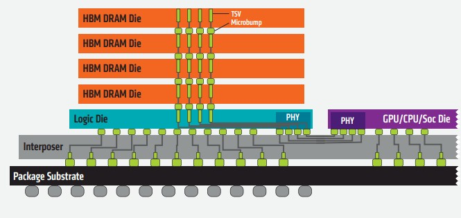
HBM is a type of computer memory that’s used in many data-intensive applications. HBM is made up of stacks of memory chips that are designed to store and transmit data quickly.
Why HBM exists
- You want massive bandwidth without cranking clock speeds to the moon.
- HBM achieves this by giving the GPU a super-wide bus (thousands of bits wide) at lower frequency.
- That wide bus is only feasible if the memory is very close to the GPU (on the same package), otherwise routing would be a nightmare.
An RTX590 doesn’t have HBM, it’s GDDR7.
HBM is Stacked on the same package as the processor (3D stacked).
- Source: https://www.nextplatform.com/2021/07/21/what-faster-and-smarter-hbm-memory-means-for-systems/
HBM memory allows for four, eight, or twelve DRAMs to be stacked atop each other and linked to each other with through-silicon vias
Do not confuse this with NVLink / Interconnect
HBM is a type of memory for your GPUs. It has nothing to do with GPU <> GPU communication. For that, it’s usually NVLINK if you’re using NVIDIA.
HBM achieves higher bandwidth than DDR4 or GDDR5 while using less power, and in a substantially smaller form factor.
This is achieved by stacking up to eight DRAM dies and an optional base die which can include buffer circuitry and test logic.
I don't see how stacking DRAM in HBM is different than putting DRAM around peripheral of CPU/GPU?
The asianometry video explains this.
Resources
- How this tiny GPU invented the Future
- The Special Memory Powering the AI Revolution by Asianometry
- https://www.tomshardware.com/reviews/glossary-hbm-hbm2-high-bandwidth-memory-definition,5889.html
- Found link from https://x.com/itsclivetime/status/1762413558036635697