Printed Circuit Board (PCB)
Video: https://www.youtube.com/watch?v=YJr-kHy6STg
Do I need to know this as a hobbyist?
According to Ethan Childerhorse, yes I do. It’s about having things in a smaller form factor, and having things that are more permanent.
I designed my first PCB back in Grade 9, but I never assembled it because I didn’t have the confidence ;(. I basically used an Arduino Uno, not very impressive to be honest.
What’s stopping me right now from designing a PCB?
- The fear of not knowing what I am doing. Okay, what do you need to learn to have more confidence on how to design a PCB?
- I want to understand how logic and circuitry works. For my VR Headset Logs, I need to understand how the MCU is integrated. Should I surface mount
I think these are notes crash course:
- Many old circuits were built used wires. Repairing circuits was also tedious.
- 1936: Paul printed conducting circuits on non conductive board.
How modern PCBs are manufactured
- start from copper flat sheet
- Laminated on insulating fibre glass
- Registration holes are drills for alignment
- Computer aided simulations to generate gerber files for drilling machines to create holes
- Board is then cleaned.
- Etching process in which board is scratched.
- dipped in alkaline solution, left only with required copper. UV process to stick mask.
- Final step: silkscreen
- Soldering components using liquid tin. Probe testing is done to test the connections
Why are PCBs green? Solder musk coating to prevent rust.
Two ways PCBs are manufactured:
- Through-Hole Technology (THT)
- Surface-Mount Technology (SMT)
PCB Manufacturing Process
There are these parallels with manufacturing an Integrated Circuit (which use wafers)
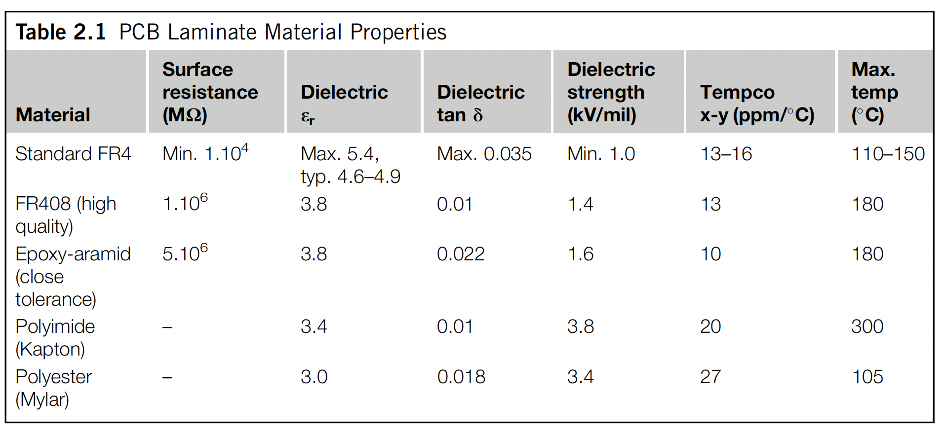
An unprocessed board is a laminate of a conductive material and an insulating dielectric substrate.
PCB Laminate Materials

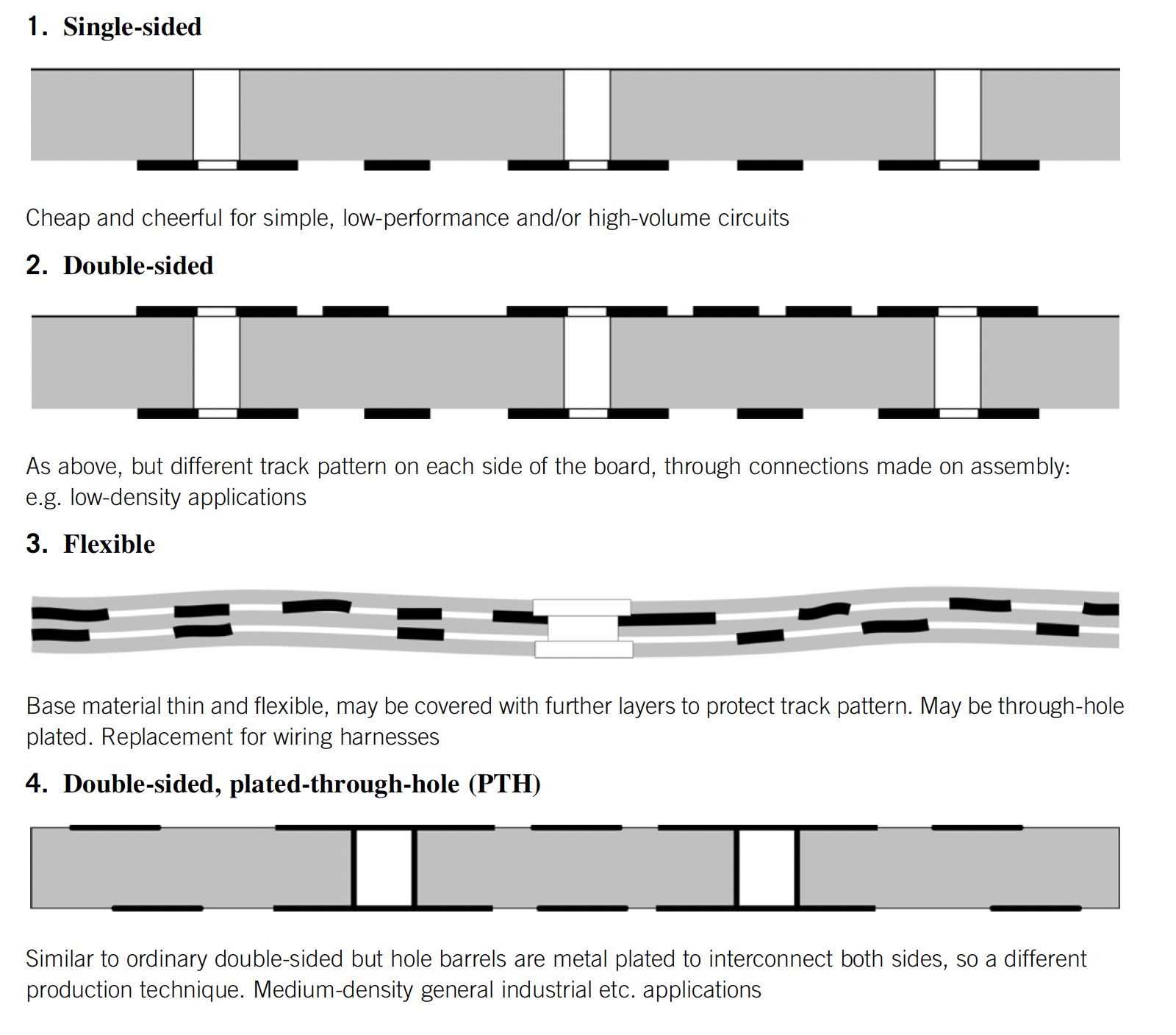
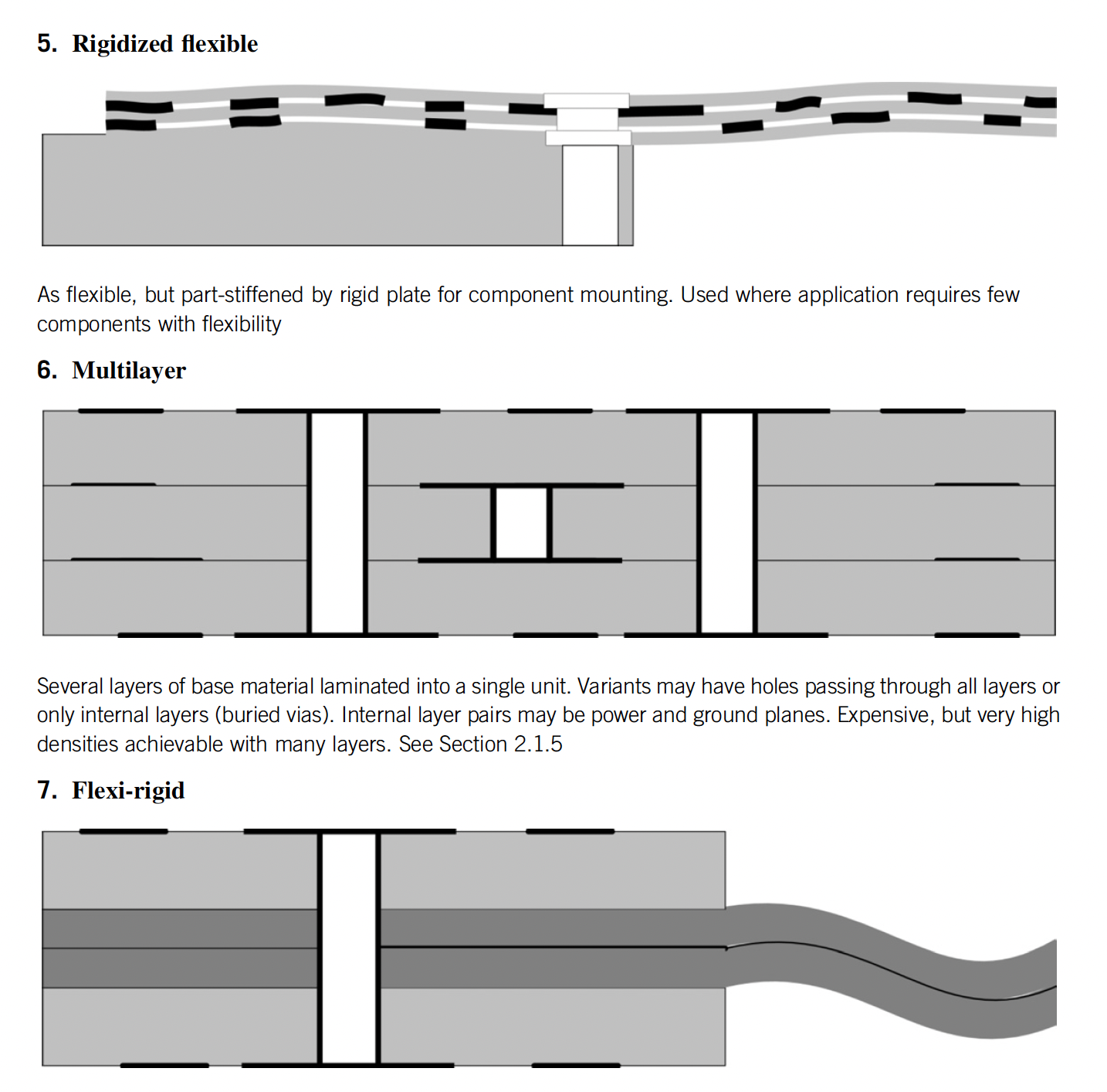
Types of Circuit constructions Most circuit requirements can be accommodated on one of the following board types, which are listed roughly by increasing cost.


How are multilayer boards actually made? IDK, to complete.
PCB Design Rules
2.2.3. Track Routing Routing is one of the most important things.
- Minimize track length so it’s less susceptible to interference and crosstalk
- Prefer 45 degree angled bends over right angles, to increase tracking density.