NVIDIA H100
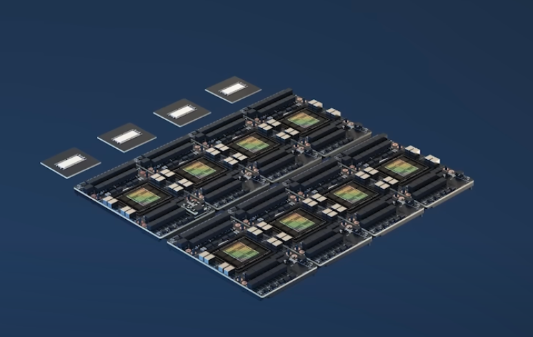
DGX H100
Each of these 8 H100 talk through NVLink.
Specs (CS231n 2025 Lec 11)
- HBM: 80GB @ 3352 GB/sec memory bandwidth.
- SMs (Streaming Multiprocessors): 132 enabled out of 144 on die.
- L1 cache per SM: 256KB.
- FP32 cores per SM: 128.
- Tensor Cores per SM: 4, each doing 4096 FLOP/cycle at bf16/fp16.
- Peak bf16 throughput (dense, sparse-free): ~989 TFLOPS on a full matmul (≈80% HFU in practice).
A100→H100 is 3.1× peak FLOPs but only 2.1× memory bandwidth — why newer devices sometimes show lower MFU even as absolute throughput goes up. Memory-bound ops (norms, softmax, optimizer) don’t scale with tensor-core FLOPs.
GPU generation timeline (peak tensor-core TFLOPs at the dominant training precision): K40 (2013) 5 → P100 (2016) 19 → V100 (2017) 125 → A100 (2020) 312 (bf16) → H100 (2022) ~1000 (bf16) → B200 (2024) 5000.
Source
CS231n 2025 Lec 11 slides ~1–20 (H100 die shot, HBM/SM/Tensor Core counts, GPU FLOPs timeline chart). 2026 PDF not published — using 2025 fallback.