P-n Junction
A p–n junction is a boundary or interface between two types of semiconductor materials, p-type and n-type, inside a single crystal of semiconductor.
Learned from Ben Eater, see Semiconductor.
Will allow current to flow in one direction, but not the other. This is exactly how a Diode works!!
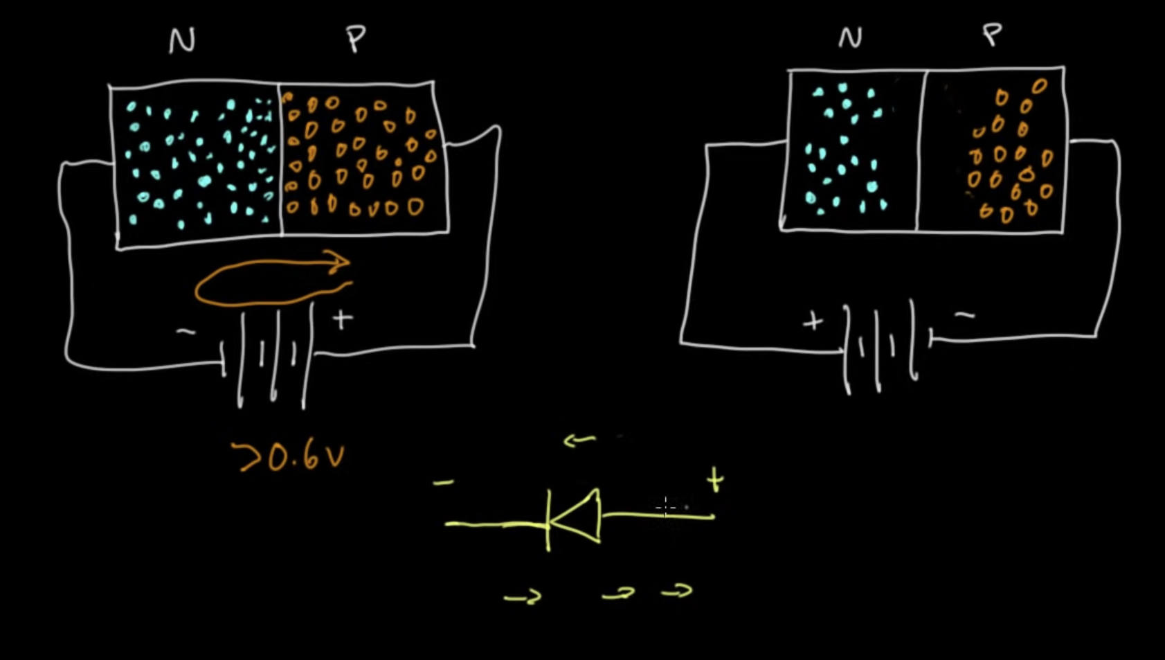
Depletion Region
In the middle (called the P-n Junction), we have what is called a depletion region.
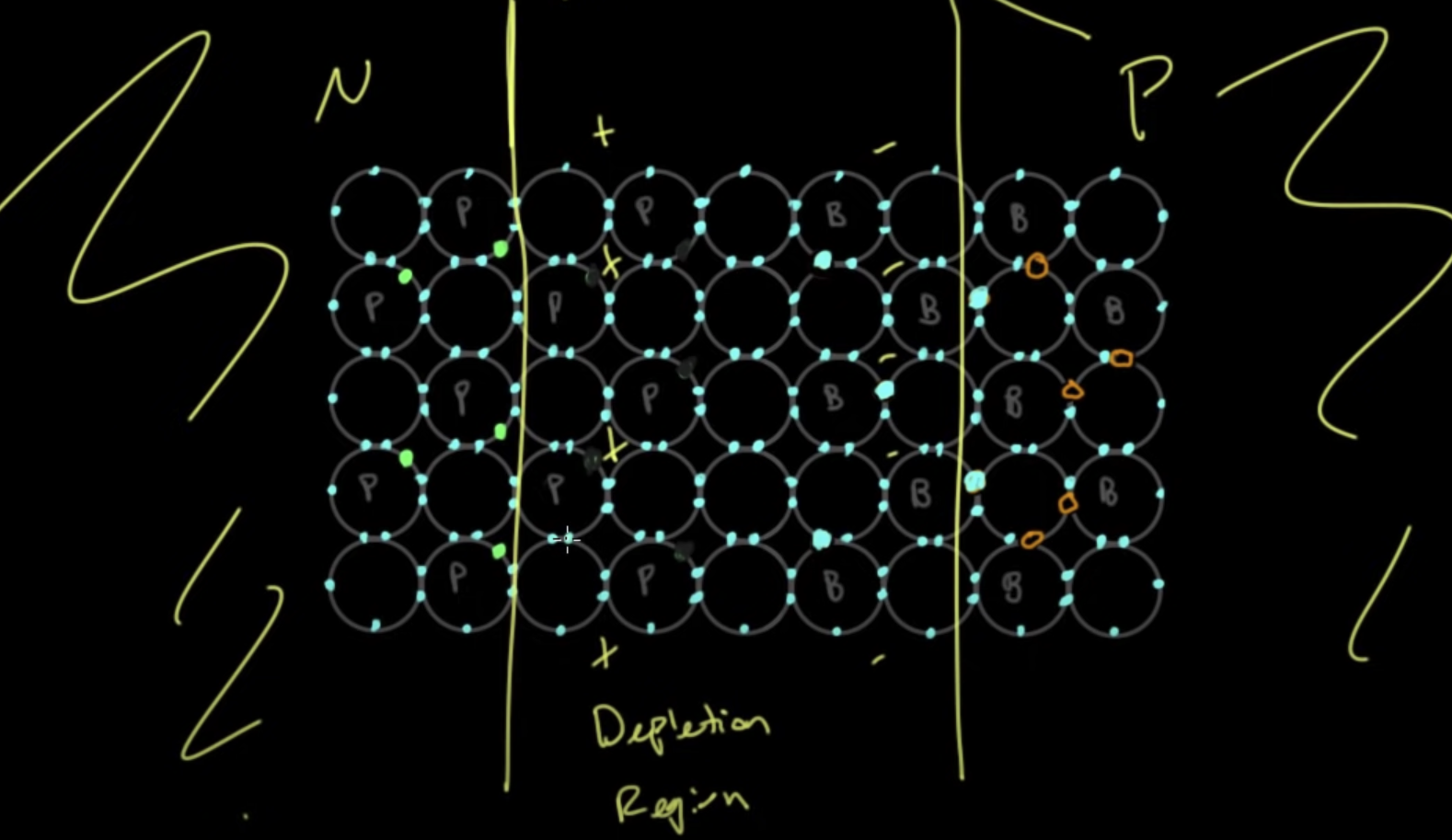
- This is fundamental to understand as this is the whole reason that Transistors can act like logic gates
In the depletion region, it sort of acts like an insulator because there is no space for the electrons to move around.
You can also watch this video starting around 3:00 to visualize the P-N Junction
Sam Zeloof Explanation
Taken from his talk.
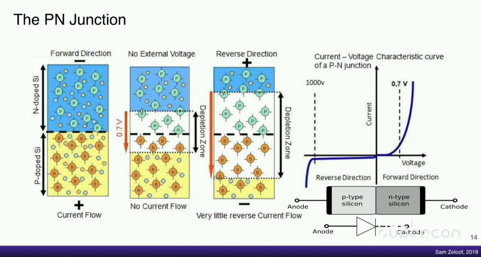
- When , more electrons.
- What’s actually going, when you put a negative voltage to a n-type region, it’s going more electrons. When you put a positive voltage to a P-type region, it’s got more holes.
- So the electrons will be pushed, the holes will be pulled, and that will be have enough energy to get through the depletion region
- If you connect the other way around, It’s going to increase the depletion region!!