RISC-V Implementation
Temporarily putting notes here, since I don’t know where to put it.
This is about how you would be how you convert RISC-V code into actual hardware, for different classes of instructions:
- Memory Reference
- load word
lw - store word
sw
- load word
- Arithmetic-logical instructions (R-Type Instructions)
add,sub,andandor
- Branches
- Conditional branch instruction
beq
- Conditional branch instruction
For every instruction, the first two steps are identical:
- Send the Program Counter (PC) to the memory that contains the code and fetch the instruction from that memory
- Read one or two registers, using fields of the instruction to select the registers to read.
After this step, the actions undertaken depends on the instruction class.
Let’s start simple and build our way to a full implementation that takes into account Clock cycles.
Below is an abstract view of the implementation of the RISC-V subset:
- Arrows = direction of information flow
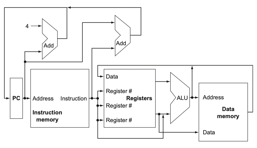
- All instructions start by using the Program Counter to supply the instruction address to the instruction memory.
- After the instruction is fetched, the register operands used by an instruction are specified by fields of that instruction.
- Once the register operands have been fetched, they can be operated on to
- compute a memory address (for a load or store)
- ALU result is used as an address to either load a value from memory into the registers or store a value from the registers. Result from the ALU or memory is written back into the register file
- compute an arithmetic result (for an integer arithmetic-logical instruction),
- Result from the ALU is written to a register
- or an equality check (for a branch)
- Use the ALU output to determine the next instruction address, which comes either from the adder (where the PC and branch offset are summed) or from an adder that increments the current PC by four.
- compute a memory address (for a load or store)
Below is the basic implementation of the RISC-V subset, including the necessary Multiplexers and control lines.
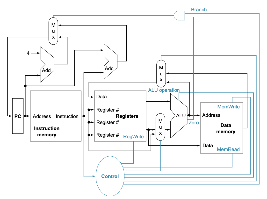
- Top multiplexor controls what value replaces the PC (PC + 4 or the branch destination address);
- Controlled by the gate that “ANDs” together the Zero output of the ALU and a control signal that indicates that the instruction is a branch.
- Middle multiplexor chooses between two outputs
- output from ALU (in the case of an arithmetic-logical instruction)
- Output from the data memory (in the case of a load) for writing into the register file.
- This output is returned to the Register File
- Bottom multiplexor is used to determine whether the second ALU input is from the registers (for an arithmetic-logical instruction or a branch) or from the offset field of the instruction (for a load or store).
- There is also a Control Unit
- Takes instruction (opcodes) as input, and determines how to set the control lines for the functional units and two of the MUX
- This makes so much sense now, the opcodes that we learn are not random gibberish. They actually mean something at the hardware level!
- Takes instruction (opcodes) as input, and determines how to set the control lines for the functional units and two of the MUX
Next up, see Datapath to learn more about the implementation for the flow of data.