Semiconductor Device Fabrication
We briefly saw this in ECE222, but this is actually SO COOL.
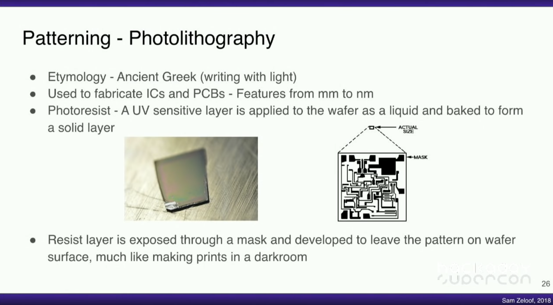
- Photoresist material
Ahh, what is explained here is directly shown in Sam’s latest video
Sams’ Hackaday talk is a really solid introduction
Fabrication techniques:
- Patterning through Photolithography
- Doping
- Layering
- This is how PCBs are made, and at a smaller scale, how ICs are made
Manufacturing an Integrated Circuit
These notes are too high level.
You should watch Sam Zeloof’s videos where he manufactures his own chips.
The manufacture of a chip begins with Silicon, a substance found in sand. Because silicon does not conduct electricity well, it is called a Semiconductor.
With a special chemical process, we add materials to silicon that allow tiny areas to transform into one of three devices:
- Excellent Conductor of electricity (using either microscopic copper or aluminum wire)
- Excellent insulator from electricity (like plastic sheathing or glass)
- Areas that can conduct or insulate under specific conditions (as a switch) → this is where Transistor come into play
- We start with a silicon crystal ingot, which looks like a giant sausage. Today, ingots are 8–12 inches in diameter and about 12–24 inches long.
- An ingot is finely sliced into Wafers no more than 0.1 inches thick.
- These wafers then go through a series of processing steps, during which patterns of chemicals are placed on each wafer, creating the transistors, conductors, and insulator
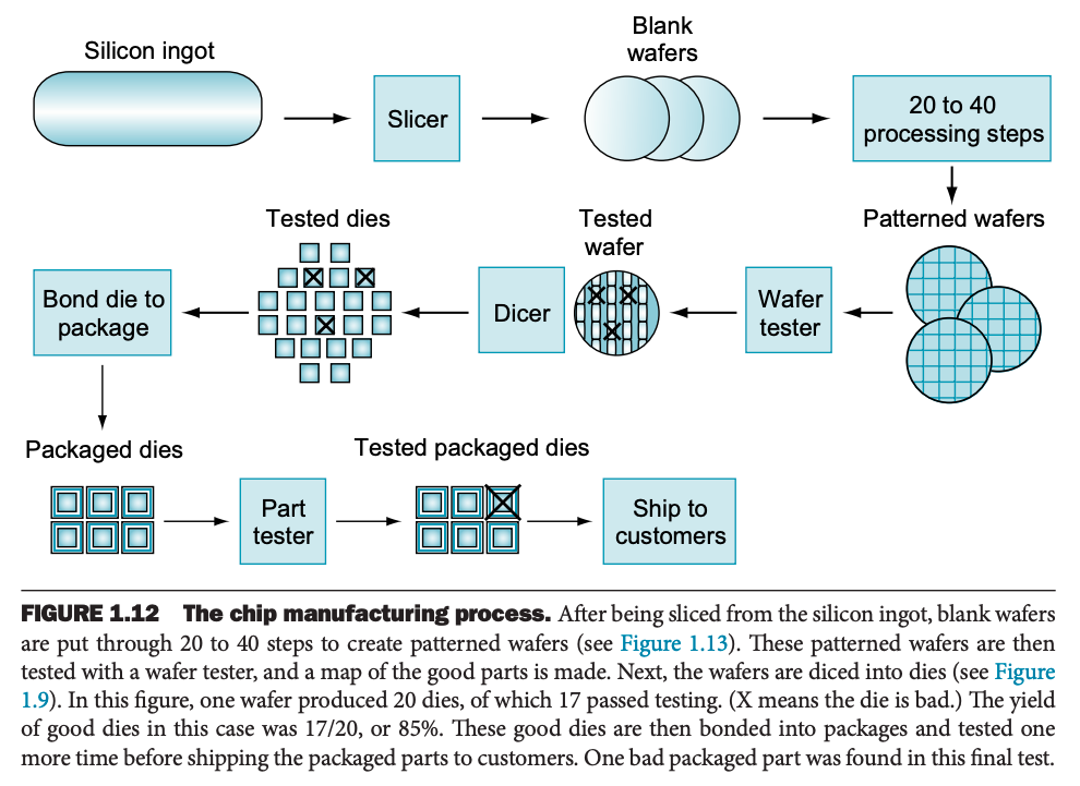
It’s really hard to manufacture a perfect chip without defects, so there is a lot of verification when we manufacture the chips.
The wafer is cut into dies.
Die
A die, in the context of integrated circuits, is a small block of semiconducting material on which a given functional circuit is fabricated.
https://www.quora.com/What-is-the-difference-between-a-wafer-and-a-die